
- Home
- Live Blog
- Breaking News
- Top Headlines
- Cities
- NE News
- Sentinel Media
- Sports
- Education
- Jobs
Sanjeev Hazarika
(sanjeev.hazarika77@gmail.com)
Of late, we have heard the term ‘semiconductors’ in the news very often. There is a sudden focus in this area with an incentive of $10 billion (about Rs 78,000 crore) from the central government and defining an India semiconductor mission. Last year, there was an international conference called ‘Semicon India 2023’ where the government invited semiconductor companies from all across the world to participate in India’s vision of semiconductor business in the near future. Following this, a lot of states, such as Gujrat, Rajasthan, UP, Karnataka,Telangana, and Assam, are coming up with their own policies in this sector. Recently, the Central government has approved three major projects in this area worth Rs 1.3 lakh crore; this includes a semiconductor assembly and test facility by TATA in Assam. Since there is a lot of focus in this direction, let us understand why there is a sudden interest in this area.
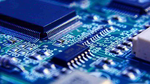
Semiconductor chips, or microchips, as they are commonly known, are the building blocks of electronic systems today. All the gadgets that we use in our day-to-day lives—whether we take our mobile phone, TV, fridge, washing machine, or computers—are all designed with a lot of microchips in them. And more and more chips are also being used in cars and bikes, military equipment, aeroplanes, and telecommunication systems. Practically, there is no aspect in which microchips do not touch our lives in some way or another. The use of microchips and powerful software gives us a better user experience when we use consumer electronics items, drive a vehicle, or fly in an aircraft. Electronic hardware combined with intelligent software has It has also enabled the government to provide better service to people, if we take the example of Aadhaar-based services or UPI (unified payment interface). It is also creating new areas of business, for example, in EdTech or e-commerce, which have a huge impact on the economies of any country. According to some estimates, the size of the consumer electronics market in India at present is about $100 billion, and it is expected to grow exponentially in the near future.
Let us understand what these microchips are. All microchips are made of a semiconductor material like silicon, whose conductivity (capacity to carry electric current) lies between a good conductor like copper or a good insulator. Using the semiconductor material, we can build an electronic switch called a transistor. This transistor is the basic building block of all microchips. Modern technology has enabled us to pack billions of transistors into a small piece of silicon. A larger number of transistors gives more computation to the microchips and allows more complex software to be built on the hardware, which has a significant impact on our day-to-day lives.
When transistors were invented, they were discrete devices. In the early 1960s, scientists and engineers invented the process of integrating large numbers of transistors into a small piece of silicon, and the ear of VLSI (Very Large-Scale Integration) was born. Fairchild Semiconductors and Intel Corporation were some of the pioneers in this field. The founder of Intel, Mr. Gordon Moore, predicted that every 18–24 months, the number of transistors that can be packed in the same size of silicon would double, which later came to be known as Moore’s law. Moore’s law became the driving force for the semiconductor industry, and we have seen scaling (the process of reducing the size of the transistors) become the norm. Every 1.5–2 years, we see a new technology (known as a process node) emerge that allows more and more transistors to be packed into the same size of silicon. This allows us to build more powerful chips that can perform more complex functions. Just to understand how scaling impacts our lives, we can compare the mobile phone 20 years ago to today’s mobile phone. What today’s phone can do was unimaginable even a few years ago.
Now let us understand where India stands in the global electronics and semiconductor landscape. We can divide the electronics industry into two parts: a) the assembly of electronics products like mobile phones, computers, TVs, fridges, etc. b) manufacturing of electronic components like microchips and display systems (display screens of phones, TVs, and other equipment). India has a huge market in terms of the electronics goods that we consume. We also have a very solid automobile industry, which is heavily dependent on the electronics industry for entertainment. GPS systems in cars use a lot of microchips. We also have a growing aerospace and military defence sector where a good number of electronic systems are used. India has done very well under ‘the’make in India’ initiative to assemble finished goods like TVs, computers, and mobile phones. We have the most advanced electronic assembly plants, including those for the Apple iPhone. However, we have very limited electronic component manufacturing facilities in India (which are mostly used for military and space applications) and import most of these components, like microchips or display systems, that are used in the assembly of electronic products. We import all these components, assemble them, and manufacture the final goods, like TVs, computers, mobile phones, etc., that we see in the shops. Most of these electronic components are manufactured in countries like Taiwan, Malaysia, Singapore, South Korea, and China. This business model was going fine for a long time, but during COVID, the supply of chips and other electronics components was disrupted as the global supply chain was badly hit. This had a huge impact on different sectors of the economy of the country. That is when the government realised that we needed to build a system to manufacture all the electronics parts, like microchips, display systems, etc., to build a self-sustaining supply chain that could support all dependent industries. That is how the semiconductor and display policy was born. It is not only India, but all major economies in the world, that have realised the importance of building chips and other electronic components so that, in the event of a disruption like COVID, there is less impact on the economy. In today’s world, it has become even more necessary to develop these technologies given the geopolitical tension between China and Taiwan. Taiwan is a tiny country and the largest producer of chips and other electronic components. If there is a long war between China and Taiwan, like the Russia-Ukraine war, it can have a huge impact on the world economy. Hence, all major economies in the world have come up with their own semiconductor policies, including India. It is high time we develop our expertise in this high-tech field and become self-reliant inthe manufacturing of electronics components.
In brief, these are the different schemes under the Semiconductor and Display Fab policy.
n Fiscal support of 50% of the project cost for all technology nodes under the scheme for setting up semiconductor fabs in India.
n Fiscal support of 50% of the project cost under the scheme for setting up display fabs.
n Fiscal support of 50% of capital expenditure under the Scheme for Setting up of Compound Semiconductors, Silicon Photonics, Sensors, and Semiconductor ATMP and OSAT Facilities in India. Additionally, target technologies under the scheme will include discrete semiconductor fabs.
For more details, please refer to the website.
https://www.meity.gov.in/esdm/Semiconductors-and-Display-Fab-Ecosystem
Now, we will discuss what these schemes mean and what kind of impact they will have on the overall economy of India. As we have discussed earlier, we are lagging behind in the manufacturing of electronics components in India, and that is an area these schemes are largely trying to address. When it comes to manufacturing, we have a state-owned manufacturing facility, SCL, or Semiconductor Laboratory (earlier known as Semiconductor Complex LTD), which is based in Chandigarh. SCL was established way back in 1984, and since then it has been in operation except for a period between 1989 and 1997 when a major fire gutted the plant. In terms of technology, it is way behind the industry. However, the chips that are manufactured here are used for internal defence and aerospace applications. The government also has plans to make this a state-of-the-art facility for the current semiconductor mission.
There is another aspect to the whole semiconductor business, and that is the design of semiconductor chips. The design of chips involves the design of all the electronic circuits that go into the silicon chip. This is a complex process that requires a lot of expertise. So, essentially, the semiconductor business consists of two verticals: chip design and chip manufacturing, both of which require different domain knowledge. Fortunately, India has been doing well in the first aspect, which is chip design. It all started in 1985, when U.S.-based Texas Instruments set up a design centre in Bengaluru. Since then, many U.S. and European-based chip design companies have set up their centres here, and now each and every global chip design company has design centres in India, mainly in Bengaluru, Hyderabad, or Noida. That is good news: we have a large pool of design engineering talent in the chip design domain. Now, the design centres in India work on complex chip designs that get manufactured in the chip manufacturing facilities in Taiwan, China, and are used in electronics products all around the world. Now, along with the MNCs that are working in this domain, India has also indigenously developed some of the designs, notably the SHAKTI processor developed by IIT Chennai or the AUM processor, which the CDAC (Centre for Development of Advanced Computing) is working on. These are good developments, and hopefully, in the near future, we will see some Indian companies competing with the MNC in the chip design space.
Now, if we look at the semiconductor policy announced by the government, there are two parts: one is an incentive for the manufacturing of semiconductor chips and display units (also packaging and testing of chips), and the other is an incentive for the design of semiconductor chips. We can call part one a production-linked incentive (PLI) and the other a design-linked incentive (DLI). Now, the question is: what is the need for providing incentives? We have discussed earlier how critical these electronic components are in different sectors of our economy. Both semiconductor design and manufacturing are capital-intensive and require a lot of money to start with. Just to give an example, to set up a chip manufacturing plant (also known as a FAB or foundry), we need anywhere around 2–3 billion dollars (about 20000 crore rupees). It also requires a lot of land, water, and electricity. Definitely, the government needs to provide some support and give incentives to encourage the private sector to establish these units. It is all the more important given the fact that we do not have the expertise in this area, and we need to attract chip manufacturing companies to India to setup FABs independently or through collaboration with Indian companies. Many chip manufacturing houses have expressed their interest in establishing these units after the government announced these schemes. The TATA Group has proposed a test and assembly facility in Assam. They are also planning to start a chip manufacturing facility in Gujarat in collaboration with Taiwan-based PSMC. US-based Micron has already started to set up a semiconductor assembly and test facility in Gujarat. Following this development, several other companies have also signed MoUs with different state governments and expressed their interest in semiconductor testing and assembly units. Another chip manufacturing facility by Tower Semiconductor from Israel is in the advanced stages of negotiations.
Similarly, the design of semiconductor chips also requires a good amount of money, as we need to go all the way up to the production of the design in manufacturing houses. Hence, there is an incentive under the policy to encourage design companies to use indigenous chip designs.
Now, the big question is: do we have the talent pool to work in this high-tech area? India has a huge engineering and science talent pool, and that is a great advantage. We already have a lot of expertise in the chip design area. Many of the US- and Europe-based chip design companies have been in operation in India for about two decades, and we have a skilled workforce in the design domain. For chip manufacturing, once the foundry is setup, people can be trained, and with the transfer of knowledge, India can build a skilled workforce in this domain over a period of time.
We hope that India’s semiconductor mission will be very successful, with a lot of design, manufacturing, testing, and packaging units in the near future. This will not only support the electronics industry but all sectors of the Indian economy. This is going to play a very critical role in India’s journey to become a developed nation.
